<< Chapter < Page Chapter >> Page >

Although, TEMs can only provide 2D analysis for a 3D specimen; magnifications of 300,000 times can be routinely obtained for many materials making it an ideal methodfor the study of nanomaterials. Besides from the TEM images, darker areas of the image show that the sample is thicker or denser in these areas, so we can observe the different components and structures of the specimen by the difference of color. For investigating multilayer-nanomaterials, a TEM is usually the first choice, because not only does it provide a high resolution image for nanomaterials but also it can distinguish each layer within a nanostructured material.

Observations of multilayer-nanomaterials

TEM was been used to analyze the depth-graded W/Si multilayer films. Multilayer films were grown on polished, 100 mm thick Si wafers by magnetron sputtering in argon gas. The individual tungsten and silicon layer thicknesses in periodic and depth-graded multilayers are adjusted by varying the computer-controlled rotational velocity of the substrate platen. The deposition times required to produce specific layer thicknesses were determined from detailed rate calibrations. Samples for TEM were prepared by focused ion beam milling at liquid N 2 temperature to prevent any beam heating which might result in re-crystallization and/or re-growth of any amorphous or fine grained polycrystalline layers in the film.

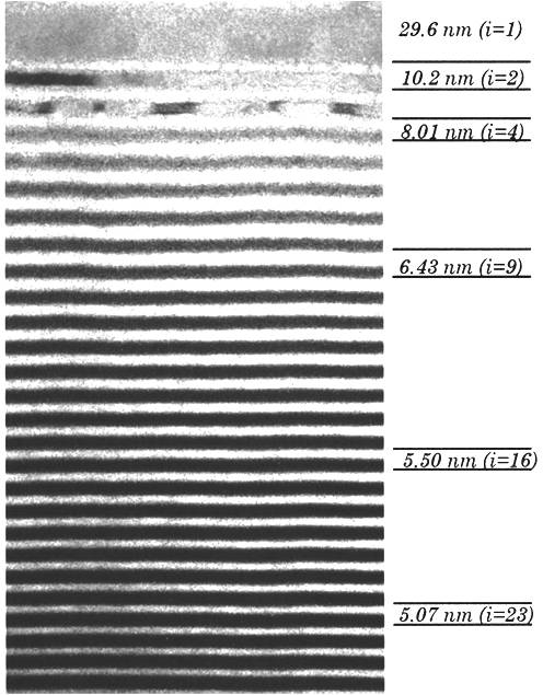
TEM measurements were made using a JEOL-4000 high-resolution transmission electron microscope operating at 400 keV; this instrument has a point-to-point resolution of 0.16 nm. Large area cross-sectional images of a depth-graded multilayer film obtained under medium magnification (~100 kX) were acquired at high resolution. A cross-sectional TEM image showed 150 layers W/Si film with the thickness of layers in the range of 3.33 ~ 29.6 nm ( [link] shows a part of layers). The dark layers are tungsten and the light layers are silicon and they are separated by the thin amorphous W–Si interlayers (gray bands). By the high resolution of the TEM and the nature characteristics of the material, each layer can be distinguished clearly with their different darkness.

Cross-sectional transmission electron micrograph of the top portion of a depth-graded W/Si multilayer structure. Selected bilayer indices and thicknesses are indicated. The tungsten (dark bands) and silicon (light bands) layers are separated by thin amorphous W–Si interlayers (gray bands). The topmost silicon layer is not completely visible in this image. Adapted from D. L. Windt, F. E. Christensen, W. W. Craig, C. Hailey, F. A. Harrison, M. Jimenez-Garate, R. Kalyanaraman, and P. H. Mao, J. Appl. Phys. , 2000, 88 , 460.

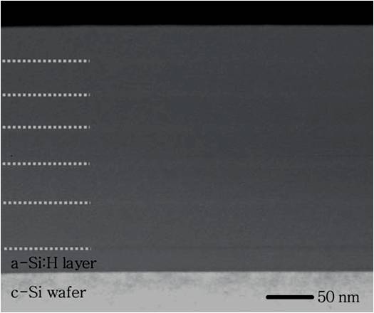
Not all kinds of multilayer nanomaterials can be observed clearly under TEM. A materials consist of pc-Si:H multilayers were prepared by a photo-assisted chemical vapor deposition (photo-CVD) using a low-pressure mercury lamp as an UV light source to dissociate the gases. The pc-Si:H multilayer included low H 2 -diluted a-Si:H sublayers (SL’s) and highly H 2 -diluted a-Si:H sublayers (SH’s). Control of the CVD gas flow (H 2 |SiH 4 ) under continuous UV irradiation resulted in the deposition of multilayer films layer by layer.

For a TEM measurement, a 20 nm thick undiluted a-Si:H film on a c-Si wafer before the deposition of multilayer to prevent from any epitaxial growth. [link] shows a cross-sectional TEM image of a six-cycled pc-Si:H multilayer specimen. The white dotted lines are used to emphasize the horizontal stripes, which have periodicity in the TEM image. As can be seen, there are no significant boundaries between SL and SH could be observed because all sublayers are prepared in H 2 gas. In order to get the more accurate thickness of each sublayer, other measurements might be necessary.

Cross-sectional TEM image of a 6-cycled pc-Si:H multilayer. Before the multilayer deposition, a 20 nm thick a-Si:H was deposited on a c-Si substrate. Adapted from S. W. Kwon, J. Kwak, S. Y. Myong, and K. S. Lim, J. Non-Cryst. Solid , 2006, 352 , 1132.

Bibliography

  • D. L. Windt, F. E. Christensen, W. W. Craig, C. Hailey, F. A. Harrison, M. Jimenez-Garate, R. Kalyanaraman, and P. H. Mao, J. Appl. Phys. , 2000, 88 , 460.
  • S. W. Kwon, J. Kwak, S. Y. Myong, and K. S. Lim, J. Non-Cryst. Solid , 2006, 352 , 1132.

Questions & Answers

how does Neisseria cause meningitis
Nyibol Reply
what is microbiologist
Muhammad Reply
what is errata
Muhammad
is the branch of biology that deals with the study of microorganisms.
Ntefuni Reply
What is microbiology
Mercy Reply
studies of microbes
Louisiaste
when we takee the specimen which lumbar,spin,
Ziyad Reply
How bacteria create energy to survive?
Muhamad Reply
Bacteria doesn't produce energy they are dependent upon their substrate in case of lack of nutrients they are able to make spores which helps them to sustain in harsh environments
_Adnan
But not all bacteria make spores, l mean Eukaryotic cells have Mitochondria which acts as powerhouse for them, since bacteria don't have it, what is the substitution for it?
Muhamad
they make spores
Louisiaste
what is sporadic nd endemic, epidemic
Aminu Reply
the significance of food webs for disease transmission
Abreham
food webs brings about an infection as an individual depends on number of diseased foods or carriers dully.
Mark
explain assimilatory nitrate reduction
Esinniobiwa Reply
Assimilatory nitrate reduction is a process that occurs in some microorganisms, such as bacteria and archaea, in which nitrate (NO3-) is reduced to nitrite (NO2-), and then further reduced to ammonia (NH3).
Elkana
This process is called assimilatory nitrate reduction because the nitrogen that is produced is incorporated in the cells of microorganisms where it can be used in the synthesis of amino acids and other nitrogen products
Elkana
Examples of thermophilic organisms
Shu Reply
Give Examples of thermophilic organisms
Shu
advantages of normal Flora to the host
Micheal Reply
Prevent foreign microbes to the host
Abubakar
they provide healthier benefits to their hosts
ayesha
They are friends to host only when Host immune system is strong and become enemies when the host immune system is weakened . very bad relationship!
Mark
what is cell
faisal Reply
cell is the smallest unit of life
Fauziya
cell is the smallest unit of life
Akanni
ok
Innocent
cell is the structural and functional unit of life
Hasan
is the fundamental units of Life
Musa
what are emergency diseases
Micheal Reply
There are nothing like emergency disease but there are some common medical emergency which can occur simultaneously like Bleeding,heart attack,Breathing difficulties,severe pain heart stock.Hope you will get my point .Have a nice day ❣️
_Adnan
define infection ,prevention and control
Innocent
I think infection prevention and control is the avoidance of all things we do that gives out break of infections and promotion of health practices that promote life
Lubega
Heyy Lubega hussein where are u from?
_Adnan
en français
Adama
which site have a normal flora
ESTHER Reply
Many sites of the body have it Skin Nasal cavity Oral cavity Gastro intestinal tract
Safaa
skin
Asiina
skin,Oral,Nasal,GIt
Sadik
How can Commensal can Bacteria change into pathogen?
Sadik
How can Commensal Bacteria change into pathogen?
Sadik
all
Tesfaye
by fussion
Asiina
what are the advantages of normal Flora to the host
Micheal
what are the ways of control and prevention of nosocomial infection in the hospital
Micheal
what is inflammation
Shelly Reply
part of a tissue or an organ being wounded or bruised.
Wilfred
what term is used to name and classify microorganisms?
Micheal Reply
Binomial nomenclature
adeolu
Got questions? Join the online conversation and get instant answers!
Jobilize.com Reply

Get Jobilize Job Search Mobile App in your pocket Now!

Get it on Google Play Download on the App Store Now


Source:  OpenStax, Nanomaterials and nanotechnology. OpenStax CNX. May 07, 2014 Download for free at http://legacy.cnx.org/content/col10700/1.13
Google Play and the Google Play logo are trademarks of Google Inc.

Notification Switch

Would you like to follow the 'Nanomaterials and nanotechnology' conversation and receive update notifications?

Ask